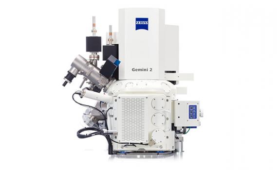
Crossbeam 550 High-Resolution Microscope

Description
ZEISS presents a new generation of focused ion beam scanning electron microscopes (FIB-SEMs) for high-end applications in research and industry. Crossbeam 550 features a significant increase in resolution for imaging and material characterization and a speed gain in sample preparation.
Nanostructures such as composites, metals, biomaterials, or semiconductors can be investigated with analytical and imaging methods in parallel. Crossbeam 550 allows simultaneous modification and monitoring of samples, resulting in fast sample preparation and high throughput.
Providing the best image quality in 2D and 3D, the Tandem decel mode enables enhanced resolution together with a maximization of image contrast at low landing energies. The pioneering Gemini II electron optics delivers optimum resolution at low voltage and high probe current simultaneously. The FIB column combines the highest available FIB current of 100 nA with the FastMill mode, allowing for highly precise and more efficient material processing and imaging in parallel.
Additionally, the new process for automated emission recovery increases user-friendliness and optimizes the FIB column for reproducible results during long-term experiments.
Material scientists profit from excellent 3D analytical properties, especially thanks to the fully integrated module for 3D EDS analyses with ZEISS Atlas 5. In the life sciences, ZEISS Crossbeam 550 convinces with its enhanced resolution at low voltages and outstanding stability for long-term 3D tomography. Moreover, it is possible to optimally integrate the new workstation into correlative workflows and to combine it with light, X-ray or ion beam microscopy.
Specs
- Gemini II optics
- Tandem decel option
- standard with 18 configurable ports or large with 22 configurable ports
- standard with 100 mm or large 153 mm travel range in x/y
- Flood Gun
- Local Charge Compensation
- Inlens SE and Inlens EsB for simultaneous imaging
- SE/EsB* imaging
- large airlock for 8 inch wafers
- configure three pneumatically driven accessories
- simultaneously on the large chamber, e.g. STEM, 4-Quadrant-Backscatter detector, and local charge compensation
- High throughput in analytics and imaging, high resolution under all conditions, simultaneous Inlens SE and Inlens EsB imaging.